Не буду вас отговаривать от желания написать всё самому. С ядром тоже если, что придётся разбираться. Но у него есть модель для ModelSim.
по конфигурационным регистрам могу дать часть кода на verilog от Lattice.
Они делают что-то подобное. Но хочу предупредить, что код был учебный и в ходе учебы его чуток подправили (мне достался уже такой).
Ядро не работало с некоторыми материнками на VIA процессоре и чипсете (Embedded) и не заводилось на некоторых современных платах с Intel Core-i3/5/7.
Поэтому перешли на PCI Mega Wizard от Altera.
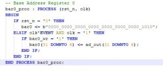
Здесь в коде по IO-map запрашивается 4К памяти. Хотя PCI от Altera ограничивает на IO всего 256 регистров.
Какие еще есть подводные камни, я не в курсе.
// --------------------------------------------------------------------
// >>>>>>>>>>>>>>>>>>>>>>>>> COPYRIGHT NOTICE <<<<<<<<<<<<<<<<<<<<<<<<<
// --------------------------------------------------------------------
// Copyright © 2001 by Lattice Semiconductor Corporation
// --------------------------------------------------------------------
//
// Permission:
//
// Lattice Semiconductor grants permission to use this code for use
// in synthesis for any Lattice programmable logic product. Other
// use of this code, including the selling or duplication of any
// portion is strictly prohibited.
//
// Disclaimer:
//
// This VHDL or Verilog source code is intended as a design reference
// which illustrates how these types of functions can be implemented.
// It is the user's responsibility to verify their design for
// consistency and functionality through the use of formal
// verification methods. Lattice Semiconductor provides no warranty
// regarding the use or functionality of this code.
//
// --------------------------------------------------------------------
//
// Lattice Semiconductor Corporation
// 5555 NE Moore Court
// Hillsboro, OR 97214
// U.S.A
//
// TEL: 1-800-Lattice (USA and Canada)
// 408-826-6000 (other locations)
//
// web:
http://www.latticesemi.com/// email: techsupport@latticesemi.com
//
// --------------------------------------------------------------------
// Revision History :
// --------------------------------------------------------------------
// Ver :| Author :| Mod. Date :| Changes Made:
// v1.0 :| D.S. :| 12/08/98 :| Initial Creation
// --------------------------------------------------------------------
//
// Module config_mux
// This block implements the PCI target configuration registers, and
// the PCI data output MUX. It controls when data gets written into the
// configuration registers, and what data gets presented onto the output
// data bus (pci_dat_out) during reads.
//
// Note: The read values for the base address registers are set in this
// block. BA0 & BA1 always return the size of the memory block for the
// backend app. when read.
//
module config_mux (pci_dat_out, ba0_size, ba1_size, bkend_dat_in,
pci_dat, pci_cbe_l, pci_addr, pci_rst_l,
abort_sig, pci_clk, com, cbe_reg_l,
idsel_reg, ba0_en, ba1_en, pci_irdy_l,
//JO ADD
ba0_rw_reg, ba1_rw_reg
//END JO ADD
);
output [31:0] pci_dat_out; // the pci output data bus
output [31:4] ba0_size; // The address space required for ba0
output [31:4] ba1_size; // The address space required for ba1
output [2:0] com; // The Mem - I/O enable bits of the command reg
output ba1_en, ba0_en;
input pci_irdy_l;
input [3:0] cbe_reg_l;
input idsel_reg;
input [31:0] bkend_dat_in; // back end data in
input [7:0] pci_addr;
input [31:0] pci_dat; // pci data
input [3:0] pci_cbe_l; // byte enables in
input pci_rst_l; // async reset
input abort_sig; // state machine is aborting set status
input pci_clk;
//JO ADD
input [31:0] ba0_rw_reg;
input [31:0] ba1_rw_reg;
//END JO ADD
/******************************************************************/
// reg declarations
reg [7:0] int_line; // r/w interupt line register
reg [31:0] pci_dat_out; // output data bus
reg [31:0] cfg_dat_out; // output data bus
reg [2:0] com; // The command register
reg stat11; // The status register bit for signaled target abort
reg stat_com_en;
reg int_line_en;
reg ba1_en;
reg ba0_en;
wire cfg_en;
reg cfg_out;
/******************************************************************/
// The following parameters set the values for the read only
// configuration registers.
/******************************************************************/
/************ Start Reg 00h Section ***************/
/******************************************************************/
// reg 00h (DevID/VendorID)
parameter DEVICE_ID = 16'hBEEF; // BEEF

))
parameter VENDOR_ID = 16'hDEAD; // DEAD
))
/******************************************************************/
/************ End Reg 00h Section *****************/
/******************************************************************/
/******************************************************************/
/************ Start Reg 04h Section ***************/
/******************************************************************/
//reg 04h (status/command)
// The only bits used in this section are status[11:9]
// Command[1:0] The rest are all disabled to 0 at the Mux inputs
// `defines used for devsel
`define fast 2'b00
`define medium 2'b01
`define slow 2'b10
parameter DEV_SEL = `medium; // medium devsel timing
// The creation of the status and Command Registers
always @ (posedge pci_clk or negedge pci_rst_l)
if (pci_rst_l == 1'b0) begin
com <= 3'b000; // disable I/O and MEM space accesses.
stat11 <= 1'b0; // reset target abort status bit
end
else if (stat_com_en == 1'b1) begin
if (!pci_cbe_l[0]) // check to see if byte lane is enabled
com <= pci_dat[2:0];
else
com <= com;
if (!pci_cbe_l[3] && pci_dat[27]) // check to see if byte lane is enabled
stat11 <= 0; // write a 1 clears this bit
else
stat11 <= stat11;
end
else if (abort_sig == 1'b1) begin
stat11 <= 1'b1; // set target abort status bit
com <= com;
end
else begin
stat11 <= stat11;
com <= com;
end
/******************************************************************/
/************ End Reg 04h Section *****************/
/******************************************************************/
/******************************************************************/
/************ Start Reg 08h Section ***************/
/******************************************************************/
// reg 08h (Class/revision)
parameter CLASS_CODE = 24'h058000; // Memory Controller
parameter REVISION_ID = 8'h01; // Rev. 01
/******************************************************************/
/************ End Reg 08h Section *****************/
/******************************************************************/
/******************************************************************/
/************ Start Reg 0Ch Section ***************/
/******************************************************************/
// reg 0Ch (Misc Functions)
// No BIST, Type 00 header, Ignore Cachelinesize, No Latency Set,
parameter MISC_FUNCTIONS = 32'h00002000;
/******************************************************************/
/************ End Reg 0Ch Section *****************/
/******************************************************************/
/******************************************************************/
/************ Start Base Address Defines Section ***************/
/******************************************************************/
// Base address registers.
// The Following `defines are used in the Base Address Parameters
// To set if the Back End Device is:
// -User I/O or Memory
// -Where it is locatated in the address map
// -If the backend device is prefetchable
// -How much address space it requires
`define MEM_ON 1'b0
`define IO_ON 1'b1
`define ANYWHERE_IN_32 2'b00
`define BELOW_1M 2'b01
`define ANYWHERE_IN_64 2'b10
`define PREFETCH_ON 1'b1
`define PREFETCH_OFF 1'b0
`define ADDR_2G 28'h8000_000
`define ADDR_1G 28'hC000_000
`define ADDR_512M 28'hE000_000
`define ADDR_256M 28'hF000_000
`define ADDR_128M 28'hF800_000
`define ADDR_64M 28'hFC00_000
`define ADDR_32M 28'hFE00_000
`define ADDR_16M 28'hFF00_000
`define ADDR_8M 28'hFF80_000
`define ADDR_4M 28'hFFC0_000
`define ADDR_2M 28'hFFE0_000
`define ADDR_1M 28'hFFF0_000
`define ADDR_512K 28'hFFF8_000
`define ADDR_256K 28'hFFFC_000
`define ADDR_128K 28'hFFFE_000
`define ADDR_64K 28'hFFFF_000
`define ADDR_32K 28'hFFFF_800
`define ADDR_16K 28'hFFFF_C00
`define ADDR_8K 28'hFFFF_E00
`define ADDR_4K 28'hFFFF_F00
`define ADDR_2K 28'hFFFF_F80
`define ADDR_1K 28'hFFFF_FC0
`define ADDR_512 28'hFFFF_FE0
`define ADDR_256 28'hFFFF_FF0
`define ADDR_128 28'hFFFF_FF8
`define ADDR_64 28'hFFFF_FFC
`define ADDR_32 28'hFFFF_FFE
`define ADDR_16 28'hFFFF_FFF
/******************************************************************/
/************ End Base Address Defines Section ***************/
/******************************************************************/
/******************************************************************/
/************ Start Reg 10h Section ***************/
/******************************************************************/
// reg 10h (Base Address 0) BA0 Using `defines from above
parameter [31:0] BA0 = {`ADDR_4K,`PREFETCH_OFF,`ANYWHERE_IN_32,`IO_ON};
assign ba0_size = BA0[31:4]; // Used to decode hit_ba0_l
/******************************************************************/
/************ End Reg 10h Section *****************/
/******************************************************************/
/******************************************************************/
/************ Start Reg 14h Section ***************/
/******************************************************************/
// reg 14h (Base Address 1) BA1 Using `defines from above
parameter [31:0] BA1 = {`ADDR_1M,`PREFETCH_OFF,`ANYWHERE_IN_32,`MEM_ON};
assign ba1_size = BA1[31:4]; // Used to decode hit_ba1_l
/******************************************************************/
/************ End Reg 14h Section *****************/
/******************************************************************/
/******************************************************************/
/************ Start Reg 2C Section ***************/
/******************************************************************/
// reg 2Ch (SubsystemID/Subsystem VendorID)
parameter SUB_SYSTEM_ID = 16'hBEEF; // Govyadina
parameter SUB_VENDOR_ID = 16'hDEAD; // Set to AMD
/******************************************************************/
/************ End Reg 2Ch Section *****************/
/******************************************************************/
/******************************************************************/
/************ Start Reg 3C Section ***************/
/******************************************************************/
// reg 3C (Max_Lat/Min_Gnt/Interrupt Pin/ Interupt Line)
// Interupt Pin is set to 1 corresponding to inta_l
parameter INT_PIN = 8'h01;
parameter MIN_GNT = 8'h2A;
// The int_line reg is defined here
// The software will write to this register
// to set the system IRQ used for the interrupt
always @ (posedge pci_clk or negedge pci_rst_l)
if (pci_rst_l == 1'b0) begin
int_line = 8'h00;
end
else if (int_line_en && !pci_cbe_l[0] ) begin // check byte enables
int_line = pci_dat[7:0];
end
else begin
int_line = int_line;
end
// Max_Lat & Min_Gnt are not implemented so they are 0's in Mux
/******************************************************************/
/************ End Reg 3Ch Section *****************/
/******************************************************************/
/******************************************************************/
/************ Start Write Enable section ***************/
/******************************************************************/
`define write_04 (pci_addr[7:0] == 8'h04)
`define write_10 (pci_addr[7:0] == 8'h10)
`define write_14 (pci_addr[7:0] == 8'h14)
`define write_3C (pci_addr[7:0] == 8'h3C)
assign cfg_en = (cbe_reg_l == 4'b1011 && idsel_reg == 1'b1) ? 1'b1 : 1'b0;
always @ (cfg_en or pci_irdy_l or pci_addr[7:0])
begin
if (cfg_en && !pci_irdy_l) begin
if (`write_04) begin
stat_com_en <= #1 1;
ba0_en <= #1 0;
ba1_en <= #1 0;
int_line_en <= #1 0;
end
else if (`write_10) begin
ba0_en <= #1 1;
stat_com_en <= #1 0;
ba1_en <= #1 0;
int_line_en <= #1 0;
end
else if (`write_14) begin
ba1_en <= #1 1;
stat_com_en <= #1 0;
ba0_en <= #1 0;
int_line_en <= #1 0;
end
else if (`write_3C) begin
int_line_en <= #1 1;
stat_com_en <= #1 0;
ba0_en <= #1 0;
ba1_en <= #1 0;
end
else begin
stat_com_en <= #1 0;
ba0_en <= #1 0;
ba1_en <= #1 0;
int_line_en <= #1 0;
end
end
else begin
stat_com_en <= #1 0;
ba0_en <= #1 0;
ba1_en <= #1 0;
int_line_en <= #1 0;
end
end
/******************************************************************/
/************ Start Output Mux Section ***************/
/******************************************************************/
always @ (posedge pci_clk or negedge pci_rst_l)
begin
if (!pci_rst_l) begin
cfg_out <= #1 1'b0;
end
else if (cbe_reg_l == 4'b1010) begin
cfg_out <= #1 1'b1;
end
else begin
cfg_out <= #1 1'b0;
end
end
always @ (cfg_dat_out or bkend_dat_in or cfg_out)
begin
if (cfg_out) begin
pci_dat_out <= #1 cfg_dat_out;
end
else
begin
pci_dat_out <= #1 bkend_dat_in[31:0];
end
end
always @ (posedge pci_clk or negedge pci_rst_l)
begin
if (!pci_rst_l) begin
cfg_dat_out <= #1 32'b0; // zero at reset
end
else begin
//JO MOD decode from pci_addr[5:2] to [7:2] (256 byte)
case (pci_addr [7:2])
6'b0000_00: cfg_dat_out <= #1 {DEVICE_ID,VENDOR_ID};// reg 00h (DevID/VendorID)
6'b0000_01: cfg_dat_out <= #1 {4'b0,stat11,DEV_SEL,9'b0,13'b0,com};//reg 04h (status/command)
6'b0000_10: cfg_dat_out <= #1 {CLASS_CODE,REVISION_ID}; // reg 08h (Class/revision)
6'b0000_11: cfg_dat_out <= #1 MISC_FUNCTIONS; // reg 0Ch (Misc Functions);
//JO MOD
//4'b01_00: cfg_dat_out <= #1 BA0; // reg 10h (Base Address 0);
6'b0001_00: cfg_dat_out <= #1 {ba0_rw_reg[31:4], 4'b1111} & BA0;
//4'b01_01: cfg_dat_out <= #1 BA1; // reg 14h (Base Address 1);
6'b0001_01: cfg_dat_out <= #1 {ba1_rw_reg[31:4], 4'b1111} & BA1;
//END JO MOD
6'b0010_11: cfg_dat_out <= #1 {SUB_SYSTEM_ID,SUB_VENDOR_ID}; // reg 2Ch (SubsystemID/Subsystem VendorID);
6'b0011_11: cfg_dat_out <= #1 {8'b0,MIN_GNT,INT_PIN,int_line}; // reg 3C (Max_Lat/Min_Gnt/Interrupt Pin/ Interupt Line);
default: cfg_dat_out <= #1 32'b0; // unimplemented return 0's;
endcase
end
end
/******************************************************************/
/************ End Output Mux Section ***************/
/******************************************************************/
endmodule //of config_mux


 Sep 18 2014, 02:05