(
источник)
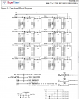
Из картинки вроде бы понятно что CS никуда не декодируются. Но что с клоками? Зачем их три штуки?
Там же объяснение
Цитата
DDR SDRAM modules operate from differential clock
inputs (CK and CK#); the crossing of CK going HIGH and
CK# going LOW will be referred to as the positive edge of
CK. Commands (address and control signals) are registered
at every positive edge of CK. Input data is registered on both
edges of DQS, and output data is referenced to both edges of
DQS, as well as to both edges of CK.
больше похоже на кусок спецификации DDR SDRAM. Этим производители чипов занимаются. На каждом чипе один клок. Как вы три дим клока подключаете к чипам, гады?


 Apr 6 2011, 09:17