| |
 Cyclone IV, стандарты IO Cyclone IV, стандарты IO, надо найти решение |
|
|
|
|
 Oct 31 2011, 08:06 Oct 31 2011, 08:06
|

Гуру

Группа: Свой
Сообщений: 2 113
Регистрация: 1-11-05
Пользователь №: 10 359

|
Разрабатывается плата, на которой имеется Cyclone4 GX 150 672FBGA в связке с OMAP-L138. А также питание и обвязка памятью.
Все интервфейсы типа DVI, CAN и прочее планируется сделать на мезонине. И вот начинаются проблемы с питанием банков:
- банк 3,4 - DDR2 1.8V
- банк 7 - DDR2 1.8V
- банк 6 - SRAM 2.5V. Тут задействованы все выводы банка на память. Единственный вопрос - позволит ли ква задействовать все выводы банка?
- банк 3A, 3B, 8A, 8B - refclk для ALTGX, 2.5В. Тут вопросов вроде бы нет, на соответсвующие входы идут LVDS клоки для GX трансмиттеров.
- банк 5, 8 - 1.8V связь с DSP (EMIF, uPP).
Мне нужно как можно больше оставшихся свободных сигналов со всех банков завести на мезонин. Но все равно не достаточно выводов для подключения, скажем DVI. Направшивающийся выход - использовать дифпары. И вот тут проблема - все банки с которых я могу взять дифпары питаются от 1.8V, а для LVDS надо 2.5В. Можно как-то это обойти?
Вопрос второй - на входы clk банков 3-8 завожу LVDS клоки. Поймет ли их плисина или при питании 1.8В нифига? Можно конечно завести с генераторов не LVDS, но не было бы проблем с шумами.
На мезонин пойдут также парочку GX-ов, но я не знаю как на мезонине без плисины преобразовать это в параллельный код...
--------------------
Быть. torizin-liteha@yandex.ru
|
|
|
|
|
|
|
 |
Ответов
|
|
Nov 1 2011, 07:07
|
Гуру
Группа: Свой
Сообщений: 2 113
Регистрация: 1-11-05
Пользователь №: 10 359
|
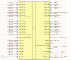
Ну вот к примеру схема включения банка 7. Как только я добавляю пин fio1 в проект (SSTL-18 или просто 1.8V), ква ругается. Но ошибка не наводит меня на суть проблемы: Цитата Error: Cannot place pin ddr2t_dq[2] to location A25
Error: Can't place VREF pin E20 (VREFGROUP_B7_N0) for pin ddr2t_dq[2] of type bi-directional with SSTL-18 Class I I/O standard at location A25
Error: Too many output and bidirectional pins per VCCIO and ground pair in I/O bank 7 when the VREF pin E20 (VREFGROUP_B7_N0) is used on device EP4CGX150DF27I7 -- no more than 9 output/bidirectional pins within 12 consecutive pads are allowed when the voltage reference pins are driving in, but there are potentially 10 pins driving out
Info: Location H17 (pad PAD_361): Pin ddr2t_a[4] of type output uses SSTL-18 Class I I/O standard
Info: Location A23 (pad PAD_362): Pin ddr2t_a[3] of type output uses SSTL-18 Class I I/O standard
Info: Location B23 (pad PAD_363): Pin ddr2t_a[2] of type output uses SSTL-18 Class I I/O standard
Info: Location D20 (pad PAD_364): Pin ddr2t_a[1] of type output uses SSTL-18 Class I I/O standard
Info: Location D21 (pad PAD_365): Pin ddr2t_a[0] of type output uses SSTL-18 Class I I/O standard
Info: Location H16 (pad PAD_366): Pin fio1 of type output uses SSTL-18 Class I I/O standard
Info: Location J16 (pad PAD_367): Pin fio0 of type output uses SSTL-18 Class I I/O standard
Info: Location E18 (pad PAD_368): Pin ddr2t_odt of type output uses SSTL-18 Class I I/O standard
Info: Location E19 (pad PAD_369): Pin ddr2t_csn of type output uses SSTL-18 Class I I/O standard
Info: Location H15 (pad PAD_370): Pin ddr2t_wen of type output uses SSTL-18 Class I I/O standard
Info: Following 12 location(s) shared the same VCCIO and ground pair, and 10 pin(s) are placed
Info: Location E20 (pad PAD_359): unused
Info: Location G17 (pad PAD_360): unused
Info: Location H17 (pad PAD_361): Pin ddr2t_a[4] of type output uses SSTL-18 Class I I/O standard
Info: Location A23 (pad PAD_362): Pin ddr2t_a[3] of type output uses SSTL-18 Class I I/O standard
Info: Location B23 (pad PAD_363): Pin ddr2t_a[2] of type output uses SSTL-18 Class I I/O standard
Info: Location D20 (pad PAD_364): Pin ddr2t_a[1] of type output uses SSTL-18 Class I I/O standard
Info: Location D21 (pad PAD_365): Pin ddr2t_a[0] of type output uses SSTL-18 Class I I/O standard
Info: Location H16 (pad PAD_366): Pin fio1 of type output uses SSTL-18 Class I I/O standard
Info: Location J16 (pad PAD_367): Pin fio0 of type output uses SSTL-18 Class I I/O standard
Info: Location E18 (pad PAD_368): Pin ddr2t_odt of type output uses SSTL-18 Class I I/O standard
Info: Location E19 (pad PAD_369): Pin ddr2t_csn of type output uses SSTL-18 Class I I/O standard
Info: Location H15 (pad PAD_370): Pin ddr2t_wen of type output uses SSTL-18 Class I I/O standard
Error: Cannot place pin ddr2t_dq[4] to location B22
Error: Can't place VREF pin E20 (VREFGROUP_B7_N0) for pin ddr2t_dq[4] of type bi-directional with SSTL-18 Class I I/O standard at location B22
Error: Too many output and bidirectional pins per VCCIO and ground pair in I/O bank 7 when the VREF pin E20 (VREFGROUP_B7_N0) is used on device EP4CGX150DF27I7 -- no more than 9 output/bidirectional pins within 12 consecutive pads are allowed when the voltage reference pins are driving in, but there are potentially 10 pins driving out
Info: Location H17 (pad PAD_361): Pin ddr2t_a[4] of type output uses SSTL-18 Class I I/O standard
Info: Location A23 (pad PAD_362): Pin ddr2t_a[3] of type output uses SSTL-18 Class I I/O standard
Info: Location B23 (pad PAD_363): Pin ddr2t_a[2] of type output uses SSTL-18 Class I I/O standard
Info: Location D20 (pad PAD_364): Pin ddr2t_a[1] of type output uses SSTL-18 Class I I/O standard
Info: Location D21 (pad PAD_365): Pin ddr2t_a[0] of type output uses SSTL-18 Class I I/O standard
Info: Location H16 (pad PAD_366): Pin fio1 of type output uses SSTL-18 Class I I/O standard
Info: Location J16 (pad PAD_367): Pin fio0 of type output uses SSTL-18 Class I I/O standard
Info: Location E18 (pad PAD_368): Pin ddr2t_odt of type output uses SSTL-18 Class I I/O standard
Info: Location E19 (pad PAD_369): Pin ddr2t_csn of type output uses SSTL-18 Class I I/O standard
Info: Location H15 (pad PAD_370): Pin ddr2t_wen of type output uses SSTL-18 Class I I/O standard
Info: Following 12 location(s) shared the same VCCIO and ground pair, and 10 pin(s) are placed
Info: Location E20 (pad PAD_359): unused
Info: Location G17 (pad PAD_360): unused
Info: Location H17 (pad PAD_361): Pin ddr2t_a[4] of type output uses SSTL-18 Class I I/O standard
Info: Location A23 (pad PAD_362): Pin ddr2t_a[3] of type output uses SSTL-18 Class I I/O standard
Info: Location B23 (pad PAD_363): Pin ddr2t_a[2] of type output uses SSTL-18 Class I I/O standard
Info: Location D20 (pad PAD_364): Pin ddr2t_a[1] of type output uses SSTL-18 Class I I/O standard
Info: Location D21 (pad PAD_365): Pin ddr2t_a[0] of type output uses SSTL-18 Class I I/O standard
Info: Location H16 (pad PAD_366): Pin fio1 of type output uses SSTL-18 Class I I/O standard
Info: Location J16 (pad PAD_367): Pin fio0 of type output uses SSTL-18 Class I I/O standard
Info: Location E18 (pad PAD_368): Pin ddr2t_odt of type output uses SSTL-18 Class I I/O standard
Info: Location E19 (pad PAD_369): Pin ddr2t_csn of type output uses SSTL-18 Class I I/O standard
Info: Location H15 (pad PAD_370): Pin ddr2t_wen of type output uses SSTL-18 Class I I/O standard
Info: Following 12 location(s) shared the same VCCIO and ground pair, and 10 pin(s) are placed
Info: Location E20 (pad PAD_359): unused
Info: Location G17 (pad PAD_360): unused
Info: Location H17 (pad PAD_361): Pin ddr2t_a[4] of type output uses SSTL-18 Class I I/O standard
Info: Location A23 (pad PAD_362): Pin ddr2t_a[3] of type output uses SSTL-18 Class I I/O standard
Info: Location B23 (pad PAD_363): Pin ddr2t_a[2] of type output uses SSTL-18 Class I I/O standard
Info: Location D20 (pad PAD_364): Pin ddr2t_a[1] of type output uses SSTL-18 Class I I/O standard
Info: Location D21 (pad PAD_365): Pin ddr2t_a[0] of type output uses SSTL-18 Class I I/O standard
Info: Location H16 (pad PAD_366): Pin fio1 of type output uses SSTL-18 Class I I/O standard
Info: Location J16 (pad PAD_367): Pin fio0 of type output uses SSTL-18 Class I I/O standard
Info: Location E18 (pad PAD_368): Pin ddr2t_odt of type output uses SSTL-18 Class I I/O standard
Info: Location E19 (pad PAD_369): Pin ddr2t_csn of type output uses SSTL-18 Class I I/O standard
Info: Location H15 (pad PAD_370): Pin ddr2t_wen of type output uses SSTL-18 Class I I/O standard
Error: Cannot place pin ddr2t_dq[6] to location C22
Error: Can't place VREF pin E20 (VREFGROUP_B7_N0) for pin ddr2t_dq[6] of type bi-directional with SSTL-18 Class I I/O standard at location C22
Error: Too many output and bidirectional pins per VCCIO and ground pair in I/O bank 7 when the VREF pin E20 (VREFGROUP_B7_N0) is used on device EP4CGX150DF27I7 -- no more than 9 output/bidirectional pins within 12 consecutive pads are allowed when the voltage reference pins are driving in, but there are potentially 10 pins driving out
Info: Location H17 (pad PAD_361): Pin ddr2t_a[4] of type output uses SSTL-18 Class I I/O standard
Info: Location A23 (pad PAD_362): Pin ddr2t_a[3] of type output uses SSTL-18 Class I I/O standard
Info: Location B23 (pad PAD_363): Pin ddr2t_a[2] of type output uses SSTL-18 Class I I/O standard
Info: Location D20 (pad PAD_364): Pin ddr2t_a[1] of type output uses SSTL-18 Class I I/O standard
Info: Location D21 (pad PAD_365): Pin ddr2t_a[0] of type output uses SSTL-18 Class I I/O standard
Info: Location H16 (pad PAD_366): Pin fio1 of type output uses SSTL-18 Class I I/O standard
Info: Location J16 (pad PAD_367): Pin fio0 of type output uses SSTL-18 Class I I/O standard
Info: Location E18 (pad PAD_368): Pin ddr2t_odt of type output uses SSTL-18 Class I I/O standard
Info: Location E19 (pad PAD_369): Pin ddr2t_csn of type output uses SSTL-18 Class I I/O standard
Info: Location H15 (pad PAD_370): Pin ddr2t_wen of type output uses SSTL-18 Class I I/O standard
Info: Following 12 location(s) shared the same VCCIO and ground pair, and 10 pin(s) are placed
Info: Location E20 (pad PAD_359): unused
Info: Location G17 (pad PAD_360): unused
Info: Location H17 (pad PAD_361): Pin ddr2t_a[4] of type output uses SSTL-18 Class I I/O standard
Info: Location A23 (pad PAD_362): Pin ddr2t_a[3] of type output uses SSTL-18 Class I I/O standard
Info: Location B23 (pad PAD_363): Pin ddr2t_a[2] of type output uses SSTL-18 Class I I/O standard
Info: Location D20 (pad PAD_364): Pin ddr2t_a[1] of type output uses SSTL-18 Class I I/O standard
Info: Location D21 (pad PAD_365): Pin ddr2t_a[0] of type output uses SSTL-18 Class I I/O standard
Info: Location H16 (pad PAD_366): Pin fio1 of type output uses SSTL-18 Class I I/O standard
Info: Location J16 (pad PAD_367): Pin fio0 of type output uses SSTL-18 Class I I/O standard
Info: Location E18 (pad PAD_368): Pin ddr2t_odt of type output uses SSTL-18 Class I I/O standard
Info: Location E19 (pad PAD_369): Pin ddr2t_csn of type output uses SSTL-18 Class I I/O standard
Info: Location H15 (pad PAD_370): Pin ddr2t_wen of type output uses SSTL-18 Class I I/O standard
Error: Cannot place pin ddr2t_dq[7] to location D22
Error: Can't place VREF pin E20 (VREFGROUP_B7_N0) for pin ddr2t_dq[7] of type bi-directional with SSTL-18 Class I I/O standard at location D22
Error: Too many output and bidirectional pins per VCCIO and ground pair in I/O bank 7 when the VREF pin E20 (VREFGROUP_B7_N0) is used on device EP4CGX150DF27I7 -- no more than 9 output/bidirectional pins within 12 consecutive pads are allowed when the voltage reference pins are driving in, but there are potentially 10 pins driving out
Info: Location H17 (pad PAD_361): Pin ddr2t_a[4] of type output uses SSTL-18 Class I I/O standard
Info: Location A23 (pad PAD_362): Pin ddr2t_a[3] of type output uses SSTL-18 Class I I/O standard
Info: Location B23 (pad PAD_363): Pin ddr2t_a[2] of type output uses SSTL-18 Class I I/O standard
Info: Location D20 (pad PAD_364): Pin ddr2t_a[1] of type output uses SSTL-18 Class I I/O standard
Info: Location D21 (pad PAD_365): Pin ddr2t_a[0] of type output uses SSTL-18 Class I I/O standard
Info: Location H16 (pad PAD_366): Pin fio1 of type output uses SSTL-18 Class I I/O standard
Info: Location J16 (pad PAD_367): Pin fio0 of type output uses SSTL-18 Class I I/O standard
Info: Location E18 (pad PAD_368): Pin ddr2t_odt of type output uses SSTL-18 Class I I/O standard
Info: Location E19 (pad PAD_369): Pin ddr2t_csn of type output uses SSTL-18 Class I I/O standard
Info: Location H15 (pad PAD_370): Pin ddr2t_wen of type output uses SSTL-18 Class I I/O standard
Info: Following 12 location(s) shared the same VCCIO and ground pair, and 10 pin(s) are placed
Info: Location E20 (pad PAD_359): unused
Info: Location G17 (pad PAD_360): unused
Info: Location H17 (pad PAD_361): Pin ddr2t_a[4] of type output uses SSTL-18 Class I I/O standard
Info: Location A23 (pad PAD_362): Pin ddr2t_a[3] of type output uses SSTL-18 Class I I/O standard
Info: Location B23 (pad PAD_363): Pin ddr2t_a[2] of type output uses SSTL-18 Class I I/O standard
Info: Location D20 (pad PAD_364): Pin ddr2t_a[1] of type output uses SSTL-18 Class I I/O standard
Info: Location D21 (pad PAD_365): Pin ddr2t_a[0] of type output uses SSTL-18 Class I I/O standard
Info: Location H16 (pad PAD_366): Pin fio1 of type output uses SSTL-18 Class I I/O standard
Info: Location J16 (pad PAD_367): Pin fio0 of type output uses SSTL-18 Class I I/O standard
Info: Location E18 (pad PAD_368): Pin ddr2t_odt of type output uses SSTL-18 Class I I/O standard
Info: Location E19 (pad PAD_369): Pin ddr2t_csn of type output uses SSTL-18 Class I I/O standard
Info: Location H15 (pad PAD_370): Pin ddr2t_wen of type output uses SSTL-18 Class I I/O standard
Info: Following 12 location(s) shared the same VCCIO and ground pair, and 10 pin(s) are placed
Info: Location E20 (pad PAD_359): unused
Info: Location G17 (pad PAD_360): unused
Info: Location H17 (pad PAD_361): Pin ddr2t_a[4] of type output uses SSTL-18 Class I I/O standard
Info: Location A23 (pad PAD_362): Pin ddr2t_a[3] of type output uses SSTL-18 Class I I/O standard
Info: Location B23 (pad PAD_363): Pin ddr2t_a[2] of type output uses SSTL-18 Class I I/O standard
Info: Location D20 (pad PAD_364): Pin ddr2t_a[1] of type output uses SSTL-18 Class I I/O standard
Info: Location D21 (pad PAD_365): Pin ddr2t_a[0] of type output uses SSTL-18 Class I I/O standard
Info: Location H16 (pad PAD_366): Pin fio1 of type output uses SSTL-18 Class I I/O standard
Info: Location J16 (pad PAD_367): Pin fio0 of type output uses SSTL-18 Class I I/O standard
Info: Location E18 (pad PAD_368): Pin ddr2t_odt of type output uses SSTL-18 Class I I/O standard
Info: Location E19 (pad PAD_369): Pin ddr2t_csn of type output uses SSTL-18 Class I I/O standard
Info: Location H15 (pad PAD_370): Pin ddr2t_wen of type output uses SSTL-18 Class I I/O standard
Error: Can't fit design in device
Error: Quartus II 64-Bit Fitter was unsuccessful. 13 errors, 4 warnings
Error: Peak virtual memory: 481 megabytes
Error: Processing ended: Tue Nov 01 09:46:56 2011
Error: Elapsed time: 00:00:06
Error: Total CPU time (on all processors): 00:00:06
Error: Peak virtual memory: 481 megabytes
Error: Processing ended: Tue Nov 01 09:46:56 2011
Error: Elapsed time: 00:00:06
Error: Total CPU time (on all processors): 00:00:06
Error: Quartus II Full Compilation was unsuccessful. 15 errors, 230 warnings Я так понимаю, что он требует, чтобы на каждые 9 последовательно (это как?) идущих пинов был хотя бы один промежуток? Что-то я не разглядел где про это написано.
Эскизы прикрепленных изображений
--------------------
Быть. torizin-liteha@yandex.ru
|
|
|
|
|
|
|
|
Nov 1 2011, 07:32
|
Частый гость
Группа: Свой
Сообщений: 181
Регистрация: 28-08-04
Пользователь №: 557
|
QUOTE (torik @ Nov 1 2011, 11:07)  Ну вот к примеру схема включения банка 7.
Как только я добавляю пин fio1 в проект (SSTL-18 или просто 1.8V), ква ругается. Но ошибка не наводит меня на суть проблемы:
Я так понимаю, что он требует, чтобы на каждые 9 последовательно (это как?) идущих пинов был хотя бы один промежуток? Что-то я не разглядел где про это написано. Quartus хочет VREF, т.к. voltage-referenced. Для предыдущих чипов была глава Pad Placement. Сейчас там пишут только: юзайте Chip Planner и будет вам счастье.
|
|
|
|
|
|
Сообщений в этой теме
 torik Cyclone IV, стандарты IO Oct 31 2011, 08:06 torik Cyclone IV, стандарты IO Oct 31 2011, 08:06 torik По первому вопросу вижу ответ (не знаю как не заме... Oct 31 2011, 09:36 EugeneS QUOTE (torik @ Oct 31 2011, 12:06) Мне ну... Oct 31 2011, 09:52 torik ЦитатаВроде бы для клоков есть VCC_CLKIN ?
Только ... Oct 31 2011, 10:04 torik По первому вопросу вижу ответ (не знаю как не заме... Oct 31 2011, 09:36 EugeneS QUOTE (torik @ Oct 31 2011, 12:06) Мне ну... Oct 31 2011, 09:52 torik ЦитатаВроде бы для клоков есть VCC_CLKIN ?
Только ... Oct 31 2011, 10:04  EugeneS QUOTE (torik @ Oct 31 2011, 14:04) Только... Oct 31 2011, 12:40 torik Печально, но ква не дает в банке, где сидят DDR2 п... Oct 31 2011, 13:59 Hoodwin А SSTL II Differential оно дает использовать вмес... Oct 31 2011, 14:18 torik SSTL только на клоковых входах-выходах. Но я погля... Oct 31 2011, 16:25 Hoodwin Ну вообще у DDR2 бывает DQS в виде differential SS... Oct 31 2011, 16:33 Hoodwin Ну это стандартные заморочки, связанные а) с огран... Nov 1 2011, 08:10 AndruB Цитата(Hoodwin @ Nov 1 2011, 12:10) Ну эт... Nov 6 2011, 19:32 Hoodwin Да, есть свойство, называется что-то вроде toggle_... Nov 6 2011, 20:05 torik ЦитатаДа, есть свойство, называется что-то вроде t... Nov 7 2011, 05:09 des00 Цитата(torik @ Nov 6 2011, 23:09) А как п... Nov 7 2011, 05:35 ViKo Цитата(torik @ Nov 7 2011, 07:09) А как п... Nov 9 2011, 13:47 Kuzmi4 Предпочитаю использовать это в QSF:
Кодset_instanc... Nov 9 2011, 14:10 torik О я я... Nov 9 2011, 16:44 EugeneS QUOTE (torik @ Oct 31 2011, 14:04) Только... Oct 31 2011, 12:40 torik Печально, но ква не дает в банке, где сидят DDR2 п... Oct 31 2011, 13:59 Hoodwin А SSTL II Differential оно дает использовать вмес... Oct 31 2011, 14:18 torik SSTL только на клоковых входах-выходах. Но я погля... Oct 31 2011, 16:25 Hoodwin Ну вообще у DDR2 бывает DQS в виде differential SS... Oct 31 2011, 16:33 Hoodwin Ну это стандартные заморочки, связанные а) с огран... Nov 1 2011, 08:10 AndruB Цитата(Hoodwin @ Nov 1 2011, 12:10) Ну эт... Nov 6 2011, 19:32 Hoodwin Да, есть свойство, называется что-то вроде toggle_... Nov 6 2011, 20:05 torik ЦитатаДа, есть свойство, называется что-то вроде t... Nov 7 2011, 05:09 des00 Цитата(torik @ Nov 6 2011, 23:09) А как п... Nov 7 2011, 05:35 ViKo Цитата(torik @ Nov 7 2011, 07:09) А как п... Nov 9 2011, 13:47 Kuzmi4 Предпочитаю использовать это в QSF:
Кодset_instanc... Nov 9 2011, 14:10 torik О я я... Nov 9 2011, 16:44
1 чел. читают эту тему (гостей: 1, скрытых пользователей: 0)
Пользователей: 0

|
|
|